Single-crystalline organolead halide perovskites possess optoelectronic properties that make them highly attractive for a range of applications including solar cells, light-emitting diodes, lasers, and photodetectors. But the growth of large, high-quality single crystals of perovskite has proved difficult. Now researchers from Shaanxi Normal University, Dalian Institute of Chemical Physics, and Xi’an Jiaotong University in China have devised a simple means of producing centimeter-sized single crystals [Liu et al., Materials Today (2018),].

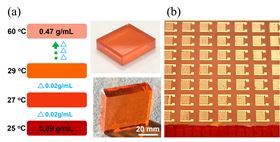
(a) Photos of MAPbBr3 single crystals grown using the LTGC process. (b) Photo of planar photodetectors based on high quality MAPbBr3 single crystals. (Image by materialstoday)
“The practical application of single-crystalline organolead halide perovskite materials is currently limited by the lack of a method for preparing high quality perovskite single crystals of large dimensions,” explains Kui Zhao, who led the research along with Shengzhong Liu.
Theoretical predictions have indicated that keeping the rate of temperature change extremely slow during growth should restrict conditions to the optimal single-crystal growth zone (OSCG). In effect, by curtailing extraneous nucleation, single crystal growth should be maximized. Now Zhao, Liu, and their colleagues have developed a low temperature-gradient crystallization (LTGC) method that can, as predicted, produce single crystals of the perovskite CH3NH3PbBr3 (MAPbBr3) over 2-inches in diameter.
“With conventional methods, the size of single crystals is limited to less than half an inch and their crystalline quality remains unsatisfactory for demanding applications,” says Zhao. “We have demonstrated well-controlled growth conditions that lie within the OSCG zone.”
The simple method starts with the mixing of precursor materials MABr and PbBr2 in a solvent for 24 hours to ensure complete dissolution. After a seed crystal is added to the solution, it is gently heated from 25°C to 60°C at a gradual rate of 2°C a day. By controlling the solute diffusion rate, very slow crystal growth minimizes the defect density, producing large and high quality single crystals after around 20 days.
“Our single crystals exhibit the best optoelectronic qualities of all MAPbBr3 materials reported in the literature, including ultralow trap state density, extremely high mobility, carrier lifetime, and diffusion length,” says Zhao.
The combination of large absorption coefficient, long electron-hole diffusion length, high carrier mobility, and superior tolerance to defects renders the single crystals particularly advantageous for optoelectronic applications.
To demonstrate the potential of the MAPbBr3 single crystals, the team created high-performance planar photodetectors with high external quantum efficiency, excellent detectivity, and fast response speed.
“To our knowledge, both the detectivity and the response speed are the best among all MAPbBr3 devices reported to date,” Zhao told Materials Today.
The team is now exploring the applicability of the growth method to other kinds of perovskite single crystals, such as ABX3 (PEA2PbI4), which could be useful for high-resolution image sensors and X-ray detectors. (materialstoday)